Saturday, 10 October 2020

Guidelines to use Zoom App (For Faculty)

Guidelines to use Zoom App (For Faculty)

Step 1:

Always Schedule the meeting. It will keep your Login link, User Id and Password same every time.  (So your saved default settings will be remain as it is)

(If you are creating New Meeting, It will not going to apply your saved default setting. Every time you have to set your required setting manually)

Step 2:  

Keep one students list in hard copy with you. Check and allow if the name and roll no is from the class only.

Keep habit of taking attendance by name only (don’t take it by Er No). Guide students to keep their DP image where face could be seen clear. (like a passport size photo)  

(Instruct Students to set their name as per the format:  Erno_name_surname 

After 5 minutes of starting make waiting room option enable. You can find in option in participants dialog box.


Step 3: Disable the option “Allow Participants to Rename Themselves“. You can find in option in participants dialog box.


Step 4: Set Chat option to “Host Only“.  You can find this option in chat dialog box.


Step 5:  If you are using screen sharing option then Disable participants annotation”. 


OR

You can keep use this option “Show Names of Annotators”


Step 6: You can share your computer sound with the students using “Share computer sound”. 


The other common guidelines you might be already aware. 

Friday, 11 September 2020

Design Voltage Follower

 Design a voltage follower (i.e., ideally voltage gain of 1).

Answer:

Voltage follower that means it follows the input voltage.

So it will be same as input signal voltage. ( Vo = Vin )

so to make this condition we have to make gain = 1 in non-inverting configuration. 

 ( Here we can not use inverting configuration because it is not possible there as its equation is   

 Here -ve sign is there )


so now let us make voltage follower from the non-inverting configuration. 


Put gain A = 1 in equation 


This says that must be 0 . Practically speaking, that means that is replaced with a shorting wire. 

What about ? Theoretically, almost any value will do. As long as there's a choice, consider infinite. Zero divided by infinite is certainly zero. 

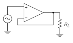
The practical benefit of choosing is that you may delete . The resulting circuit is shown in Figure.

4.2.4.png

This is how we can make voltage follower. 

Op-Amp Example 3

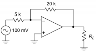
 Determine the output voltage for the circuit in Figure .

4.2.9.png

First of all here check for the type of the circuit. ( Inverting or Non-Inverting ? )

Here from the circuit, input is given to the - ve input terminal so It is Inverting configuration

So using the equation 

first i will find the gain 

Now to find the output voltage  

Here from the figure you can find the Vin value 


Op-amp example 2

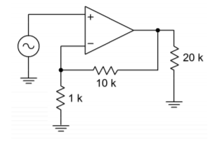
 What is the value of  gain of the circuit mentioned below

4.2.2.png


First of all here check for the type of the circuit. ( Inverting or Non-Inverting ? )

Here from the circuit, input is given to the +ve input terminal so It is Non-Inverting configuration

So using the equation 


Gain is 11. 

Op-amp Example 1

Op-amp Example 

Find the closed loop gain of the following inverting amplifier circuit.

inverting op-amp circuit

Solution: 

First of all here check for the circuit. ( is it inverting or non-inverting ?)

Here input is at the -ve terminal so it is inverting configuration.


Using the formula for the gain of the inverting op-amp circuit

inverting op-amp gain

we can now substitute the values of the resistors in the circuit as follows,

Rin = 10kΩ  and  Rƒ = 100kΩ

and the gain of the circuit is calculated as: -Rƒ/Rin = 100k/10k = -10

Therefore, the closed loop gain of the inverting amplifier circuit above is given -10 or 20dB (20log(10)).

Saturday, 5 September 2020

નોઇસ ફેક્ટર અને નોઇસ ફિગર

 નોઇસ ફેક્ટર અને નોઇસ ફિગર


કોઈ પણ એમ્પ્લીફાયર નો નોઇસ ફેક્ટર એ ઇનપુટ નો સિગ્નલ ટુ નોઇસ રેશિઓ અને આઉટપુટ નો સિગ્નલ ટુ નોઇસ રેશિઓ દ્વારા માપવામાં આવે છે .


તેનું સમીકરણ 


અહીં સિસ્ટમ ને રૂમ ટેમ્પરેચર પર ગણવામાં આવે  છે.


ઇનપુટ નો S/R રેશિઓ એ આઉટપુટ ના S/R રેશિઓ કરતા વધારે હશે. કારણ કે ઇનપુટ અને આઉટપુટ વચ્ચે એમ્પ્લીફાયર માં નોઇસ એડ થાય છે.


આમ અહીં નોઇસ ફેક્ટર એ એડ થતા નોઇસ ની વેલ્યુ બતાવે છે, જે હંમેશા ૧ કરતા વધુ છે.

નોઇસ ફેક્ટર ની આઇડલ વેલ્યુ ૧ છે.


નોઇસ  ફેક્ટર એ ઘણી વખત ફ્રીક્વન્સી પર  પણ આધારિત હોય છે. અહીં કોઈ એક ફ્રીક્વન્સી માટે નોઇસ ફેક્ટર માપવામાં આવે છે  જે સ્પોટ નોઝ ફેક્ટર તરીકે ઓળખાય છે.


નોઇસ ફિગર


જયારે નોઇસ ફેક્ટર ને ડેસીબલ માં માપવામાં આવે તો તેને નોઇસ ફિગર કહેવાય  છે.


નોઇસ ફિગર ની આઇડલ વેલ્યુ ૦ (શૂન્ય) છે


નોઇસ ફિગર ને ઈમ્પ્રુવ કરવા માટે

  • રીસીવર, એમલીફાયર ના કમ્પોનન્ટ અને મિક્ષર ઓછા નોઇસ ઉત્પન્ન કરે એવા સિલેક્ટ કરો

  • ફેટ અને ડાયોડ નો ઉપયોગ કરવો

  • રીસીવર ને ઓછા તાપમાન પર ઓપરેટ કરવા

  • વધુ ગેઇન વાળા એમ્પ્લીફાયર વાપરો 


સિગ્નલ ટુ નોઇસ રેશિઓ

 સિગ્નલ ટુ નોઇસ રેશિઓ


સિસ્ટમ માં નોઇસ ખુબ વધે નહિ એટલે કોઈ એક પોઇન્ટ પાર સિગ્નલ અને નોઇસ પાવર ને માપવામાં આવે છે.


આ સિગ્નલ પાવર અને નોઇસ પાવર ના રેશિઓ ને સિગ્નલ ટુ નોઇસ રેશિઓ SNR કહેવામાં આવે છે.


તેનું  સમીકરણ


સિગ્નલ ટુ  નોઇસ રેશિઓ  dB માં માપવામાં આવે છે.


સિસ્ટમ નું પરફોર્મન્સ સારું રાખવા માટે SNR ની વેલ્યુ  વધારે હોવી જોઈએ. ( કારણ કે સારી સિસ્ટમ માટે નોઇસ ઓછો હોવો જોઈએ.. હવે આપેલા સમીકરણ માં નોઇસ પાવર ની વેલ્યુ ઘટાડાતા  SNR  ની વેલ્યુ વધે છે )


dB  માં સમીકરણ લખવા માટે એની તરફ log વડે ગુણવું પડે


SNR  ને દરેક પરિસ્થિતિ અને કન્ડિશન માં હાઈ વેલ્યુ પર રાખવાના  પ્રયત્ન થવા  જોઈએ. 


આજ  સમીકરણ ને  વોલ્ટેજ  ની ટર્મ માં લખવા માટે


પ્રેક્ટિકલ માં ઘણી  વખત SNR  ને બદલે SINAD માપવામાં આવે છે.

જેનું સમીકરણ આ મુજબ છે


વ્હાઇટ ગોસિઅન નોઇસ

 વ્હાઇટ ગોસિઅન નોઇસ


વ્હાઇટ ગોસિઅન નોઇસ એ રેન્ડોમ સિંગ્નલ જેની ઇન્ટેન્સિટી બધી જ અલગ અલગ ફ્રીક્વન્સી માં સરખી હોય છે, જેને કારણે એક કોસ્ટન્ટ પાવર સ્પેક્ટ્રલ ડેન્સિટી જોવા મળે છે. 


વ્હાઇટ નોઇસ માં દરેક ફ્રીક્વન્સી કમ્પોનન્ટ સરખા પ્રમાણ માં હોય છે . જે વ્હાઇટ લાઈટ જેવું છે જેમાં બધા જ વિઝિબલ સ્પેક્ટ્રલ કોમ્પોનન્ટ નું મિશ્રણ હોય છે.


વ્હાઇટ નોઇસ ને ગોસિઅન ડિસ્ટ્રીબ્યુશન  આકાર હોય છે. એટલે કે વ્હાઇટ નોઇસ નો પાવર ડિસ્ટ્રીબ્યુશન ફંક્શન  નો આકાર ગોસિઅન ટાઈપ નો છે  તેથી તેને ગોસિઅન નોઇસ કહે છે.


પાવર સ્પેક્ટ્રલ ડેન્સિટી  ઓફ વ્હાઇટ નોઇસ નીચે ના સમીકરણ વડે દર્શાવાય છે.


વ્હાઇટ નોઇસ નું ઉદાહરણ: થર્મલ નોઇસ

ઇન્ટર્નલ નોઇસ ના પ્રકાર

 ઇન્ટર્નલ નોઇસ ના પ્રકાર 


ફંડામેન્ટલ નોઈસ ના કારણે અલગ-અલગ પ્રકારના નોઇસ ઉત્પન્ન થાય છે જેમકે

1.થર્મલ નોઈસ

2. શોટ નોઇસ  

3. પાર્ટીશન નોઇસ

4. લો ફ્રીક્વન્સી એટલે કે ફ્લિકર નોઇસ

5. હાઈ ફ્રીક્વન્સી એટલે કે ટ્રાન્ઝિટ ટાઈમ નોઇસ


  1. શોટ નોઇસ  


શોટ નોઇસ એ શોટ ઇફેક્ટને કારણે ઉત્પન્ન થાય છે.


આ નોઇસ એ દરેક એમ્પ્લીફાયર ડિવાઇસમાં જોવા મળે છે.


શોટ નોઇસ એ એમ્પ્લીફાયર ડિવાઈસના આઉટપુટ  ઇલેક્ટ્રોડ પર ઇલેક્ટ્રોન ના અનિયમિતપણે આવવાના કારણે થાય છે. તેને કારણે  એમ્પ્લીફાયર ના મુખ્ય આઉટપુટમાં રેન્ડમલી બદલતો નોઇસ  મુખ્ય અવાજ સાથે જોવા મળે છે.


તેનો અવાજ કોઈ મેટલ સીટ ઉપર ટાંચણી નો વરસાદ થતો હોય તેવો આવે છે.


  1.  પાર્ટીશન નોઇસ


જ્યારે કરંટ ડિવાઇડ બે કરતા વધારે રસ્તાઓમાં વિભાજીત થાય છે ત્યારે જોવા મળે છે.એ ડિવિઝન વખતે થતાં રેન્ડમ ફ્લક્ચ્યુએશન ના કારણે જોવા મળે છે બીપી તેથી જ પાર્ટીશન નોઇસ એ ડાયોડ કરતા ટ્રાન્ઝિસ્ટર માં વધુ જોવા મળે છે. 


ગેલિયમ આર્સેનાઇડ FET માં આ નોઇસ ખુબજ ઓછો જોવા મળે છે. 


  1.  લો ફ્રીક્વન્સી એટલે કે ફ્લિકર નોઇસ. 


ફ્લિકર નોઇસ એ અમુક કિલો હર્ટઝ કરતા ઓછી ફ્રીક્વન્સી માં જોવા મળે છે એને 1/F  નોઇસ  પણ કહે છે.


સેમિકન્ડક્ટર ડિવાઇસમાં કેરિયર ડેન્સિટી ની ફ્લક્ચ્યુએશન ના કારણે આ નોઇસ ઉત્પન્ન થાય છે. 


આ કેરિયર ડેન્સિટી ની ફ્લક્ચ્યુએશન ને કારણે  મટિરિયલની કન્ડક્ટિવિટી માં બદલાવ લાવે છે જેને કારણે ફ્લક્ચ્યુઍટીંગ વોલ્ટેજ ડ્રોપ ઉત્પન્ન થાય છે.આ ફ્લક્ચ્યુઍટીંગ વોલ્ટેજ ને ફ્લિકર નોઇસ કહે છે.


  1. થર્મલ નોઈસ


    થર્મલ નોટિસને જ્હોન્સન નોઈસ પણ કહેવાય છે.


કંડકટર માના ફ્રી ઇલેક્ટ્રોન હંમેશા રેન્ડમલી હરફર કરતા હોય છે, આ રેન્ડમ હરફર એ થર્મલ એનર્જી ના કારણે હોય છે. આ ફરતા ઇલેક્ટ્રોન નું કંડકટર માં ડિસ્ટ્રીબ્યુશન કોઈપણ સમયે યુનિફોર્મ/સમાંતર  હોતું નથી.


એવું પણ બની શકે છે કે ઘણા બધા ઇલેક્ટ્રોન કંડકટર ના કોઈ એક ભાગમાં જોવા મળે. આ નોન યુનિફોમ મુમેન્ટ ના કારણે એવરેજ વોલ્ટેજ  ઝીરો હોય છે પરંતુ એવરેજ પાવર ઝીરો હોતો નથી અને  અહીં આ પાવર થર્મલ એનર્જી માંથી ઉદભવે છે તેથી તેને થર્મલ નોઇસ પાવર કહે છે.


એવરેજ થર્મલ પાવર માટે  નું  સમીકરણ


    Pn=kTB Watts


    k= Boltzmann’s constant = 1.3810-23Joules/Kelvin.

    B= નોઇસ સ્પેક્ટ્રમ ની બેન્ડવિથ

    T = ટેમ્પરેચર ઓફ કન્ડકટર, Kelvin

આ  સમીકરણ ઉપર થી એવું  સિદ્ધ થાય છે કે અનંત તાપમાન પર ઓપરેટ થતા કંડક્ટર માં ઈલેકટ્રીકલ જનરેટર જેવું કામ કરે છે.


  1. હાઈ ફ્રીક્વન્સી એટલે કે ટ્રાન્ઝિટ ટાઈમ નોઇસ


ટ્રાન્ઝિટ સમય  એટલે કે કરંટ ના વાહક એવા ઇલેક્ટ્રોન કે હોલ ને ઇનપુટ થી આઉટપુટ સુધી પહોંચતા લાગતો સમય. 


ઇલેક્ટ્રોનિક  કમ્પોનન્ટ ખુબ નાના  હોય છે અને તેમના કરંટ વાહક પાથ તો એથી પણ નાના હોય છે. ઓછી ફ્રીક્વન્સી માં આ વહન સમય સારી રીતે મૈનટૈન થતો હોય છે પરંતુ હાઈ ફ્રીક્વન્સી માટે એ ડિફિકલ્ટ બને  છે. જેને કારણે એ એક નોઇસ તરીકે વર્તન કરે છે, જે  ફ્રીક્વન્સી વધવા ને સાથે 6  dB per octave ના દર થીવધે છે.


હાઈ ફ્રિકવનસી માં ઝડપી ફેરફાર ને કારણે આઉટપુટ કરંટ માં એ નોઇસ ઉત્પન્ન કરે છે.


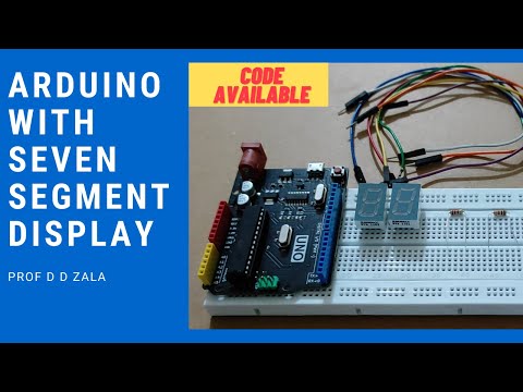
LAB 7 Arduino with Seven Segment Display || Arduino Tutorial || Code and Circuit Diagram || Project

  LAB 7 Arduino with Seven Segment Display || Arduino Tutorial || Code and Circuit Diagram || Project Dear All We will learn how to Connec...